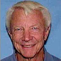
SPINDT CHARLES A. “CAPP” Dies at 92
Capp Spindt was born in San Jose, California on 20 July 1931, and raised in the small farming community of Los Banos, California. His higher education began in the School of Architecture at the University of California, Berkeley; but was interrupted by the Korean War. He joined the Air Force and entered pilot training, which he completed just as the armistice was signed. He then served as an all-weather fighter-interceptor pilot during the height of the cold war with Russia, and this experience working with the latest high-tech jet aircraft and electronics lead to a keen interest in engineering. As a result, he studied electronics after completing his Air Force service and received a BS Degree in Electrical Engineering from the California State University at San Jose in 1961. In 1990 the Eurotechnical Research University awarded him a Ph.D. degree based on his pioneering contributions to the field of Vacuum Microelectronics.
In 1959 he joined the staff of the Applied Physics Lab of the Stanford Research Institute (now SRI International) as a Student Engineer, and upon receiving his BSEE degree he became a Research Engineer working on the Vacuum Microelectronics program in SRI’s Applied Physics Lab. Since that time he has been engaged in research on thin-film deposition and micromachining technology, ultra-high vacuum processes, microchannel electron multipliers, high-density information-storage devices, and the development of three-dimensional nanofabrication technology and devices based on that technology, such as low-voltage field ionizers for nonfragmenting mass spectrometry of large molecular-weight compounds. As a part of these activities, in 1966 he invented and developed processes for fabricating the nanometer-scale, gated, field-emitter-array cathode, now commonly known as the Spindt cathode. These micro-scale emitters produce field emission at less than 100 volts compared to thousands of volts for conventional field emitters, and they have been shown to be a very efficient cold cathodes capable of producing over a thousand amps per square centimeter from close-packed arrays of tips, and pulsed emission of over a milliamp from single tips. This has been the enabling technology that led to the emergence of a new technical field dedicated to the application of microfabrication techniques to vacuum devices, and a rekindled interest in vacuum devices within the scientific community. The most notable of these devices was the field-emission flat-panel display, which was the brightest available and was worked on by several companies throughout the world (e.g. Sony, Motorola, Samsung, Raytheon, etc.). This work was published in 1968 in the Journal of Applied Physics and his image made the cover of the Journal. His breakthrough and achievement laid the Conor stone of Vacuum Microelectronics.
Dr. Spindt retired in 2002, and was a Director Emeritus of the Vacuum Microelectronics Program in the Micro Science and Engineering Laboratory at SRI. In 1992 he was named an SRI Fellow, and was inducted into the SRI Hall of Fame in 2004. He was co-founder and co-chairman of the First Institute of Electrical and Electronics Engineers (IEEE) International Vacuum Microelectronics Conference (IVMC, now the IVNC) in Williamsburg VA (1988) and chairman of the Third IVMC held in Monterey, CA (1990). He was a life member of the International Steering Committee for the IVNC. He also served on the IEEE International Vacuum Electronics Conference Committee. In 1991 he served as chairman of the Vacuum Electronics Subcommittee for the IEEE International Electron Devices Meeting in Washington, DC, and in 1993 as Vice-chairman of the IVMC in Newport, RI. He served as chairman of the IEEE International Conference on Plasma Sciences’ Vacuum Microelectronics sessions for 1998 and 1999. In 1994 and 1995 he served as a guest lecturer on vacuum microelectronics at the University of California. In 1996 he was awarded the Society for Information Display’s Jan Rajchman Prize “For the invention and development of Field-Emission Flat-Panel Displays using micro-tip structures.” He served as a guest editor for the IEEE Transactions on Electron Devices in 1988 and 1990, He has authored and co-authored over 150 papers for technical journals and scientific symposia. In addition, he has given numerous invited lectures in the United States as well as in ten other countries including a week as a guest lecturer at the National Academy of Sciences in Beijing, China. His inventions have resulted in 15 issued U.S. patents and several patents pending. He was a member the American Vacuum Society and a Life Fellow of the IEEE.
Over the years Capp received many awards from different organizations recognizing his technical contributions. What those awards do not recognize and reflect is the kind, friendly and humble man that he was to all of us. We will certainly miss him. Thank you.